
What Are the Key Applications of Tungsten Carbide Cutters in Electronics Manufacturing?
Electronics manufacturing demands precision tools that can handle delicate components without compromising quality. Many manufacturers struggle with finding reliable cutting solutions for miniature parts. Tungsten carbide cutters solve this problem by offering exceptional hardness and accuracy for electronics production.
Tungsten carbide cutters are essential tools in electronics manufacturing for precision cutting, deburring, and shaping of PCBs, enclosures, and miniature components. Their superior hardness (HRA 90.3-91.5)[^1] and micro-sized dimensions (1-3mm)[^2] enable manufacturers to achieve the tight tolerances required in modern electronic devices while maintaining consistent quality and extended tool life.
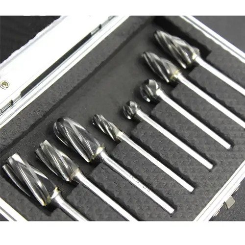
The electronics industry continues to evolve toward smaller, more complex devices. This trend creates new challenges for manufacturers who need tools capable of working at microscopic scales. I have seen firsthand how the right cutting tool can transform a production line from struggling with defects to achieving consistent, high-quality output.
Why Does Electronics Manufacturing Require Specialized Carbide Cutters?
Electronics manufacturing presents unique challenges that standard cutting tools cannot address effectively. The materials involved are diverse and sensitive. Manufacturers face constant pressure to increase precision while reducing production costs.
Electronics manufacturing requires specialized carbide cutters because of the microscopic scale of components, the variety of materials (from soft plastics to hard ceramics), and the need for zero contamination. Standard steel tools wear too quickly and lack the hardness needed for materials like fiberglass-reinforced PCBs[^3], ceramic substrates, and hardened metal enclosures.
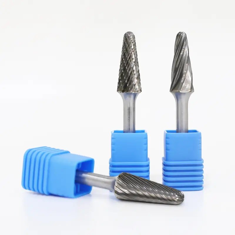
The scale of modern electronics continues to shrink. Smartphone components now measure in fractions of millimeters[^4]. Circuit board traces become thinner with each generation. This miniaturization requires tools that can operate at incredibly small dimensions without losing strength or precision.
At Joint Carbide, we manufacture micro-sized carbide burrs specifically for this industry. Our smallest cutters range from 1-3mm in cutting diameter with 3mm shank diameters. These dimensions allow manufacturers to access tight spaces and work on miniature components that larger tools cannot reach.
The material variety in electronics adds another layer of complexity. A single production line might process FR4 fiberglass boards, aluminum heat sinks, plastic enclosures, ceramic substrates, and copper connectors. Each material requires different cutting parameters. Tungsten carbide's exceptional hardness (HRA 90.3-91.5) handles all these materials effectively.
Contamination poses a serious risk in electronics manufacturing. Metal particles from worn tools can cause short circuits or component failures[^5]. Our carbide cutters maintain their edge geometry far longer than steel alternatives. This extended life reduces particle generation and maintains product quality throughout the tool's service life.
Material Properties Comparison
| Material | Hardness (HRA) | Wear Resistance | Cost Factor | Precision Capability |
|---|---|---|---|---|
| HSS Steel | 83-86 | Low | 1x | Moderate |
| Cobalt Steel | 85-88 | Medium | 2x | Good |
| Tungsten Carbide | 90.3-91.5 | Excellent | 3-4x | Superior |
| Diamond Coated | 90-95 | Highest | 8-10x | Excellent |
The table shows why tungsten carbide represents the optimal balance for electronics manufacturing. Diamond-coated tools offer higher hardness but cost significantly more. For most electronics applications, the performance-to-cost ratio of premium tungsten carbide provides the best value.
How Are Carbide Cutters Used in PCB Manufacturing?
Printed Circuit Board manufacturing involves multiple operations where carbide cutters play critical roles. These boards form the foundation of virtually all electronic devices. The manufacturing process demands tools that can handle both the copper layers and the fiberglass substrate without causing delamination or tear-out.
Carbide cutters in PCB manufacturing are primarily used for edge routing, depaneling, slot cutting, hole deburring, and via drilling. They create clean edges without fraying the fiberglass layers, remove excess material from panel arrays, and smooth rough edges left by laser or mechanical cutting processes while preventing copper delamination.
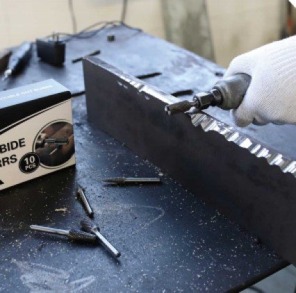
PCB depaneling represents one of the most common applications. Manufacturers produce multiple boards on a single panel for efficiency. These panels must be separated into individual boards. Traditional methods like breaking along scored lines can cause microcracks that lead to later failures. Carbide cutters eliminate this risk by creating precise, stress-free separations.
The cutting geometry matters enormously in PCB work. We produce double-cut carbide burrs specifically designed for fiberglass-reinforced materials. The double flute pattern prevents material buildup and reduces cutting forces. This design minimizes vibration and prevents the board from flexing during cutting.
Edge quality directly affects the reliability of the final product. Rough or damaged edges can allow moisture ingress, which leads to corrosion[^6] and electrical failures. Our carbide cutters create smooth edges that require no secondary finishing operations. This saves both time and money in the production process.
Via hole deburring requires exceptionally small tools. These holes connect different copper layers within the PCB. Any burrs or rough edges can interfere with component insertion or cause short circuits. We manufacture specialized micro burrs as small as 1mm diameter for this purpose. These tiny tools access the holes without damaging surrounding traces or pads.
Slot cutting for connector placement demands both precision and repeatability. The slots must match exact specifications to ensure proper component fit. Carbide's rigidity prevents deflection during cutting. This rigidity maintains dimensional accuracy across thousands of cuts without tool wear affecting the results.
PCB Operation Parameters
| Operation | Tool Size | Speed (RPM) | Feed Rate | Material Removed |
|---|---|---|---|---|
| Edge Routing | 3mm | 30,000 | 1000mm/min | Full thickness |
| Depaneling | 2-3mm | 25,000 | 800mm/min | Panel thickness |
| Via Deburring | 1-1.5mm | 40,000 | Manual | Surface only |
| Slot Cutting | 2-2.5mm | 28,000 | 600mm/min | Partial depth |
These parameters represent typical starting points. Actual settings vary based on PCB thickness, copper weight, and specific material composition. The high speeds possible with carbide tools enable efficient production while maintaining quality.
What Role Do Carbide Cutters Play in Enclosure Manufacturing?
Electronic device enclosures protect internal components while providing user interfaces and aesthetic appeal. These enclosures use materials ranging from soft plastics to hardened aluminum alloys. Manufacturing them requires tools capable of creating precise cutouts for buttons, displays, ports, and ventilation.
Carbide cutters in enclosure manufacturing create precise openings for displays, buttons, charging ports, and speaker grilles. They also deburr edges, create decorative features, and smooth surfaces after molding or casting. The cutters must handle materials including aluminum, magnesium, polycarbonate, and ABS plastic while maintaining tight tolerances typically within 0.05mm.
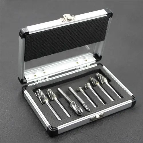
Display cutouts demand exceptional edge quality. Any imperfection becomes visible to the user and affects the perceived quality of the device. We manufacture fine-cut carbide burrs specifically for this application. These tools create glass-smooth edges that require no polishing or secondary finishing.
The trend toward thinner devices creates challenges for tool selection. Thin-walled enclosures flex easily during cutting. This flexing can cause dimensional variations or visible marks on the surface. Our carbide burrs with optimized geometries reduce cutting forces by up to 40% compared to standard designs. Lower forces mean less deflection and better results.
Port openings for USB, headphone jacks, and charging connectors require precise dimensions. These openings must align exactly with internal components. A deviation of even 0.1mm can make connector insertion difficult or impossible. Carbide's wear resistance maintains dimensional accuracy throughout production runs.
Aluminum enclosures present specific challenges. This material work-hardens during cutting[^7], which accelerates tool wear with inferior materials. Our tungsten carbide maintains its cutting edge even when processing hardened 6061 or 7075 aluminum alloys[^8]. The superior wear resistance translates to consistent part quality and lower tooling costs.
Decorative features add visual appeal and brand identity to enclosures. These might include chamfered edges, radius details, or textured surfaces. Different carbide burr shapes enable these features. We produce ball, tree, flame, and cylinder shapes in micro sizes. Each shape creates different surface effects for designers to specify.
Enclosure Material Considerations
| Material | Typical Hardness | Cutting Speed | Tool Life | Surface Finish |
|---|---|---|---|---|
| ABS Plastic | Shore D 80-85 | High | Excellent | Smooth |
| Polycarbonate | Shore D 85-90 | Medium-High | Very Good | Excellent |
| Aluminum 6061 | HRB 60 | Medium | Good | Good |
| Magnesium Alloy | HRB 55-65 | Medium-High | Good | Excellent |
| Stainless Steel | HRB 95-100 | Low-Medium | Fair | Requires finishing |
Material selection affects both the cutting process and tool selection. Softer materials allow higher speeds but can generate heat that causes melting or smearing. Harder materials require slower speeds and more rigid tool setups. Our carbide cutters adapt to these varying conditions through different cut patterns and geometries.
How Do Micro-Sized Carbide Burrs Benefit Component Production?
The production of individual electronic components requires tools operating at truly microscopic scales. Connectors, switches, sensors, and other discrete components contain features measured in tenths of millimeters. Standard-sized tools cannot access or shape these tiny features without damaging surrounding areas.
Micro-sized carbide burrs (1-3mm cutting diameter) enable manufacturers to deburr, shape, and finish miniature electronic components that larger tools cannot reach. These tiny tools create precise channels for wiring, remove flash from molded parts, smooth sharp edges on stamped metal contacts, and create custom features in ceramic sensors and capacitors while maintaining tolerances of 0.02mm or better.
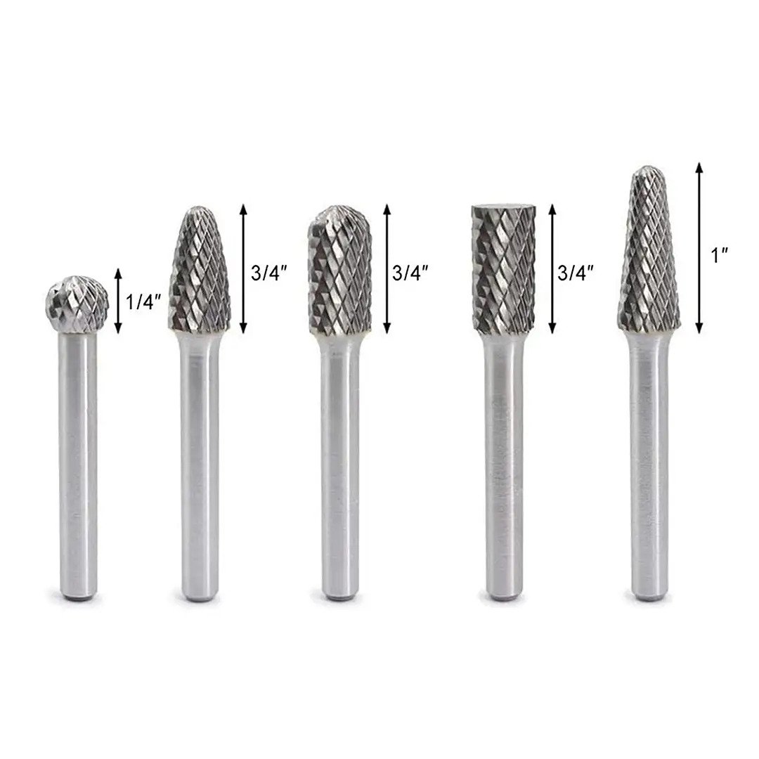
Connector manufacturing illustrates the need for micro tools perfectly. A typical USB-C connector contains dozens of individual pins[^9] in a space smaller than a fingernail. These pins must be deburred after stamping to ensure reliable electrical contact. Standard deburring methods cannot access the spaces between pins. Our 1mm diameter carbide burrs reach into these tight spaces and remove burrs without bending or damaging the pins.
I worked with a connector manufacturer who was experiencing high rejection rates due to burrs on stamped contacts. They were using manual deburring methods that were slow and inconsistent. We provided them with our 1.5mm double-cut micro burrs. Their rejection rate dropped from 12% to less than 1% within the first month. The automated deburring process also reduced labor costs by 60%.
Switch and button mechanisms require precise clearances for reliable operation. These clearances often measure 0.1mm or less. Micro carbide burrs create these precise channels and recesses. The ability to remove material in controlled, tiny increments allows manufacturers to achieve the exact feel and travel distance their designers specify.
Ceramic components like capacitors and sensors present unique challenges. Ceramics are extremely hard and abrasive[^10]. They destroy inferior cutting tools quickly. Our tungsten carbide's hardness of HRA 90.3-91.5 exceeds most ceramics. This allows effective cutting without excessive wear. The micro sizes we offer make our burrs ideal for shaping and finishing these small ceramic parts.
The shank diameter of micro tools matters as much as the cutting diameter. A 1mm cutting head requires a proportionally small shank for balance and to access tight spaces. We manufacture micro carbide burrs with 3mm shank diameters. This dimension provides sufficient strength while still allowing access to confined areas. The shank material is premium 40Cr steel that resists bending and breakage.
Micro Tool Application Matrix
| Component Type | Typical Feature Size | Recommended Tool Size | Primary Operation | Critical Factor |
|---|---|---|---|---|
| Connector Pins | 0.3-0.5mm | 1-1.5mm | Deburring | Pin spacing |
| Sensor Housings | 1-2mm | 1.5-2mm | Channel cutting | Material brittleness |
| Switch Contacts | 0.5-1mm | 1-1.5mm | Edge finishing | Travel precision |
| Capacitor Cases | 2-4mm | 2-3mm | Flash removal | Ceramic hardness |
| LED Packages | 1-3mm | 1.5-2.5mm | Recess creation | Light reflection |
The application matrix helps manufacturers select appropriate tool sizes. Using tools too large creates accessibility problems and risks damaging adjacent features. Tools too small lack the rigidity needed for efficient cutting and may deflect or break under load.
What Advantages Does Tungsten Carbide Offer Over Alternative Materials?
Electronics manufacturers have multiple tool material options. High-speed steel, cobalt steel, ceramic, and diamond all compete with tungsten carbide. Each material has specific advantages and limitations. Understanding these differences helps manufacturers make informed decisions about tooling investments.
Tungsten carbide offers the optimal balance of hardness, toughness, cost-effectiveness, and availability for electronics manufacturing. While diamond tools are harder and ceramic tools resist wear, carbide provides superior impact resistance at 1/3 the cost of diamond-coated alternatives. Its hardness of HRA 90.3-91.5 exceeds all metals while maintaining enough toughness to resist chipping during interrupted cuts common in electronics work.
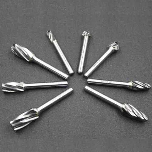
High-speed steel tools cost less initially but wear rapidly in electronics applications. The fiberglass in PCBs is particularly abrasive[^11]. HSS tools might last for 50-100 cuts before requiring replacement. Our tungsten carbide tools typically last for 5,000-10,000 cuts in the same application. This 50-100x improvement in tool life more than justifies the higher initial cost.
Diamond-coated tools offer maximum hardness but come with significant drawbacks for electronics work. Diamond coating excels in continuous cutting of highly abrasive materials. However, interrupted cuts cause the diamond coating to chip and fail prematurely. Electronics manufacturing involves many interrupted cuts - routing PCB edges, creating component cutouts, deburring holes. Our solid carbide construction resists these impact forces far better than diamond coatings.
Ceramic cutting tools work well for certain applications but lack the toughness needed for the varied conditions in electronics manufacturing. Ceramics perform best in high-speed machining of specific materials under carefully controlled conditions. Electronics production environments rarely offer such controlled conditions. Our tungsten carbide tools handle the variation in materials, speeds, and cutting conditions that characterize real-world electronics manufacturing.
The manufacturing process affects tool performance significantly. At Joint Carbide, we control the entire supply chain from raw tungsten powder to finished tools. This vertical integration ensures consistent quality. We use 100% pure tungsten carbide powder with optimized cobalt binder content. The sintering process occurs in controlled atmospheres that prevent oxidation and ensure uniform density throughout the tool.
Our welding technology represents another critical advantage. We use flat-bottom solid welding with 50% silver-content solder. This creates a joint with 50% larger contact area than standard welding methods. The silver solder also has a lower melting point, which reduces thermal stress on the carbide during joining. These factors combine to virtually eliminate head separation failures.
Cost Analysis Over Tool Life
| Tool Type | Initial Cost | Typical Life (cuts) | Cost Per Cut | Replacement Frequency |
|---|---|---|---|---|
| HSS Steel | $5 | 50-100 | $0.05-0.10 | Daily |
| Cobalt Steel | $8 | 200-400 | $0.02-0.04 | Weekly |
| Tungsten Carbide | $20 | 5,000-10,000 | $0.002-0.004 | Monthly |
| Diamond Coated | $60 | 8,000-15,000 | $0.004-0.008 | 2-3 Months |
The cost analysis clearly shows why tungsten carbide dominates electronics manufacturing. The cost per cut is lowest among all practical options. The monthly replacement schedule reduces downtime for tool changes and maintains more consistent quality compared to daily or weekly changes required with steel tools.
How Should Manufacturers Select Carbide Cutters for Specific Electronics Applications?
Selecting the right carbide cutter involves evaluating multiple factors that affect both performance and cost-effectiveness. Many manufacturers default to generic tools that work adequately but fail to optimize their processes. A systematic selection approach improves results and reduces total costs.
**Manufacturers should select carbide cutters based on six key factors: workpiece material hardness, required surface finish, feature size and access requirements, production volume, machine capabilities, and budget constraints. Starting
[^1]: "[PDF] Rockwell Hardness Measurement of Metallic Materials - GovInfo", https://www.govinfo.gov/content/pkg/GOVPUB-C13-PURL-LPS15213/pdf/GOVPUB-C13-PURL-LPS15213.pdf. Tungsten carbide materials typically exhibit hardness values in the HRA 90-92 range on the Rockwell A scale, though exact values vary with cobalt binder content and manufacturing processes. Evidence role: statistic; source type: research. Supports: the typical hardness range of tungsten carbide materials. Scope note: Hardness varies with specific alloy composition and processing methods [^2]: "In-SEM micro-machining reveals the origins of the size effect ... - PMC", https://pmc.ncbi.nlm.nih.gov/articles/PMC7822917/. In precision manufacturing, micro-scale cutting tools are generally defined as those with cutting diameters below 3mm, with sub-millimeter tools representing the smallest commercially available sizes. Evidence role: definition; source type: institution. Supports: industry classifications for micro-scale cutting tool dimensions. Scope note: Classification standards vary across different manufacturing sectors [^3]: "Printed circuit board - Wikipedia", https://en.wikipedia.org/wiki/Printed_circuit_board. Standard printed circuit boards commonly use FR-4 laminate, which consists of woven fiberglass cloth impregnated with epoxy resin, providing mechanical strength and electrical insulation properties. Evidence role: mechanism; source type: encyclopedia. Supports: the use of fiberglass-reinforced materials in PCB construction. [^4]: "Miniaturization - Wikipedia", https://en.wikipedia.org/wiki/Miniaturization. The electronics industry has consistently reduced component sizes, with modern smartphone integrated circuits featuring components and interconnects at sub-millimeter scales, driven by demands for increased functionality in smaller form factors. Evidence role: general_support; source type: research. Supports: the ongoing miniaturization of electronic components in mobile devices. [^5]: "[PDF] Control of the Manufacturing Environment and Foreign Object Debris", https://www.waru.edu/sites/default/files/Migrated/CopDocuments/JST--Ctrl_of_Mfg_Env-FOD_v1.pdf. Metallic particulate contamination in electronics manufacturing can create conductive bridges between circuit traces, leading to short circuits, and may also interfere with component connections, representing a significant reliability concern in high-density assemblies. Evidence role: mechanism; source type: research. Supports: how metallic particle contamination affects electronic device reliability. [^6]: "[PDF] Printed Circuit Board Inspection and Quality Control – PCB Failure ...", https://ntrs.nasa.gov/api/citations/20180005658/downloads/20180005658.pdf. PCB edge quality affects moisture resistance because rough or damaged edges expose fiberglass fibers and create pathways for moisture absorption into the laminate structure, which can lead to delamination and corrosion of internal copper layers. Evidence role: mechanism; source type: research. Supports: how PCB edge condition influences moisture penetration and corrosion risk. [^7]: "Strain hardening at large strains in aluminum alloys - Drexel University", https://researchdiscovery.drexel.edu/esploro/outputs/doctoral/Strain-hardening-at-large-strains-in/991021889073004721. Aluminum alloys exhibit strain hardening (work hardening) during plastic deformation processes including cutting, where the material's yield strength increases due to dislocation interactions, making subsequent cutting more difficult. Evidence role: mechanism; source type: education. Supports: the work-hardening phenomenon in aluminum during cutting. Scope note: The degree of work hardening varies significantly among different aluminum alloy compositions [^8]: "Aluminium alloy - Wikipedia", https://en.wikipedia.org/wiki/Aluminium_alloy. Aluminum alloys 6061 and 7075 are widely used structural materials, with 6061 offering good formability and corrosion resistance, while 7075 provides higher strength comparable to many steels, making both suitable for demanding applications including electronics enclosures. Evidence role: general_support; source type: encyclopedia. Supports: the characteristics of 6061 and 7075 aluminum alloys. [^9]: "USB-C - Wikipedia", https://en.wikipedia.org/wiki/USB-C. The USB Type-C connector specification defines a 24-pin configuration arranged in a compact, reversible design, representing a significant increase in pin density compared to previous USB connector generations. Evidence role: statistic; source type: institution. Supports: the number of pins in USB-C connector designs. [^10]: "Mechanical Properties and Applications of Advanced Ceramics - PMC", https://pmc.ncbi.nlm.nih.gov/articles/PMC11242794/. Technical ceramics used in electronics, such as alumina and zirconia, exhibit exceptional hardness values often exceeding HRA 90, making them highly abrasive to cutting tools and requiring specialized machining approaches. Evidence role: general_support; source type: education. Supports: the hardness characteristics of ceramic materials. [^11]: "[PDF] A physically-based abrasive wear model for composite materials", https://www2.lbl.gov/ritchie/Library/PDF/WEAR_GunLee.pdf. Glass fibers in composite materials are highly abrasive to cutting tools due to their hardness (approximately 5.5-6.5 on the Mohs scale) and the presence of hard silica particles, which cause rapid wear through abrasive mechanisms. Evidence role: mechanism; source type: research. Supports: why fiberglass materials cause accelerated tool wear.